Quantifying Initial Contact Resistance Baseline Degradation in High Frequency Sockets
Initial contact resistance degradation in RF test sockets increases insertion loss and alters impedance matching, requiring dry-circuit Kelvin monitoring.

Scrub
High-frequency IC test socket pins establish electrical continuity through microscopic contact points known as a-spots. When an integrated circuit package is loaded into a test socket, mechanical actuation drives spring probes or elastomeric columns against package balls or flat pads. Initial baseline resistance is established primarily by the lateral wiping motion designed into the pin tip architecture.
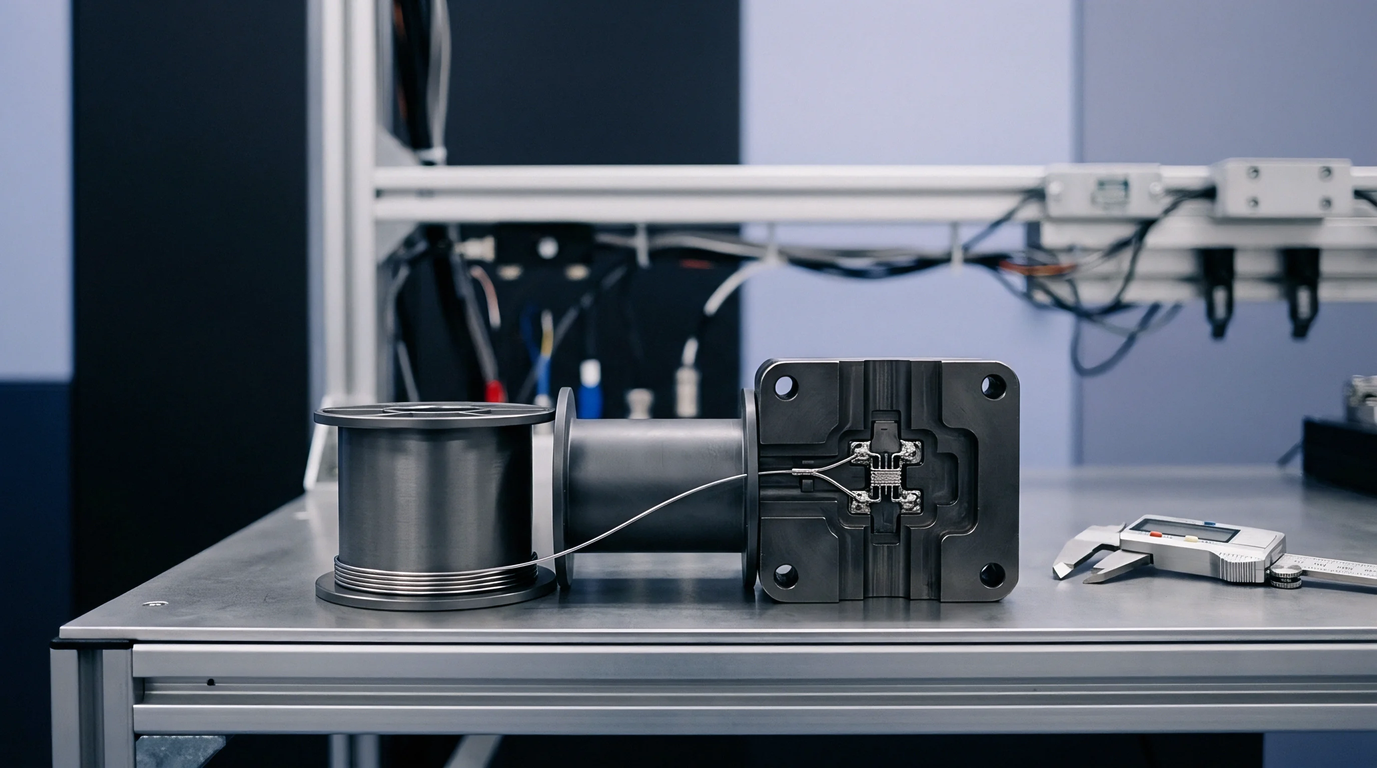
Asperity Deformation and Initial Resistance Mechanics
Clean metallic surfaces make physical contact across tiny surface peaks covering less than one percent of the nominal wipe area. Applied mechanical force crushes these asperities, breaking ambient oxide films and inducing local plastic deformation. The true contact area expands until local material yield stress balances the applied spring force, setting initial contact resistance based on material resistivity, hardness, and force.
Solid mechanical contact requires sufficient normal force to pierce ambient contaminant films.
A 15-gram actuating force on a 50-micrometer radius beryllium-copper plunger produces an initial contact resistance between 12 and 18 milliohms under ambient room conditions.
Spring probes achieve this force through internal helical springs, whereas elastomeric matrix contactors rely on compressed conductive particles embedded in silicone columns. Initial baseline contact resistance ranges from 10 milliohms in pristine spring contacts to 50 milliohms in high-density conductive elastomer arrays. Variations in initial pin force produce immediate baseline spreads across multi-pin sockets, affecting high-speed digital and RF power delivery lines.
Micro-Wipe Dynamics in High Density Socket Matrices
Spring-loaded pogo pins and elastomeric contact elements rely on sliding action to shear surface oxides during actuation. Plunger tips feature chisel, crown, or biased spear geometries to generate between 25 and 75 micrometers of horizontal scrub across the target pad, clearing debris and exposing unoxidized bulk metal.
Excessive wipe distance cuts deep grooves into device solder balls or land pads, generating loose metallic particulates that collect inside the socket guide plate. Insufficient wipe fails to break native oxide layers, causing initial contact resistance values to double or triple. Early resistance spikes often stem from mechanical plating breakdown within the pin cavity rather than device ball contamination.

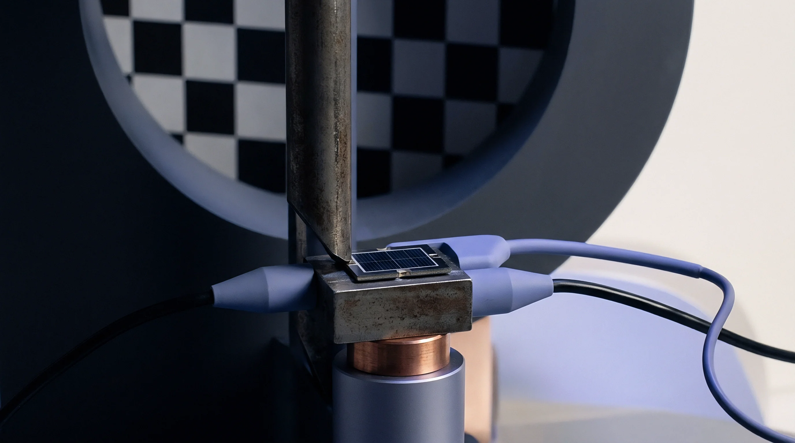
Metallurgy
Electroplated gold layers applied over nickel diffusion barriers form the primary conductive path in RF spring probes. Beryllium-copper or brass substrates supply mechanical resilience and spring memory. The outer gold layer provides low electrical resistivity and corrosion resistance, while the underlying nickel barrier blocks copper atoms from migrating into the gold film.
Fretting Wear and Interdiffusion Dynamics
Repeated actuation strips soft gold layers, exposing underlying nickel to atmospheric oxygen and moisture. Small-amplitude cyclic motion driven by thermal expansion or test handler vibration accelerates fretting wear, producing metallic debris that oxidizes into an insulating powder at the contact interface.
On a spring pin featuring a 0.76-micrometer gold layer over a 1.27-micrometer nickel barrier on a beryllium-copper core, repeated cycling reduces gold thickness by approximately 0.008 micrometers per thousand actuations under a 15-gram load. By 50,000 actuations, outer gold coverage drops below 30 percent, leaving nickel exposed to room atmosphere. The resulting nickel oxide increases interface contact resistance from an initial 15 milliohms to over 140 milliohms.
| Actuation Count | Gold Plating Thickness (µm) | Exposed Nickel Area (%) | Mean Resistance (mΩ) | Standard Deviation (mΩ) |
|---|---|---|---|---|
| 0 | 0.76 | 0.0 | 14.2 | 1.1 |
| 10,000 | 0.68 | 2.1 | 16.8 | 1.8 |
| 25,000 | 0.51 | 12.4 | 28.5 | 4.2 |
| 50,000 | 0.23 | 54.7 | 86.1 | 18.3 |
| 100,000 | 0.04 | 91.2 | 242.0 | 64.5 |
Thermal Acceleration of Intermetallic Oxide Growth
Operating temperatures around 105 degrees Celsius accelerate atomic migration between substrate copper and surface plating layers. Thermal stress during active burn-in or high-temperature operational life screening drives solid-state diffusion, causing copper atoms to migrate through the nickel barrier and oxidize upon reaching the outer gold surface.
This thermal diffusion creates resistive copper oxide films directly within the conductive path, causing contact resistance to rise non-linearly over time during extended burn-in cycles.
- Hard Gold Deposit Thickness Minimum 0.76 micrometers cobalt-hardened gold limits abrasive pin wear across 100,000 actuations.
- Sulfamate Nickel Barrier Quality A dense barrier layer prevents copper migration toward the outer contact surface under elevated burn-in temperatures.
- Beryllium Copper Substrate Temper Heat-treated alloy retaining spring force prevents mechanical relaxation under continuous mechanical deflection.
Ignoring intermetallic diffusion rates during elevated-temperature screening leads to false test rejections and inflated scrap costs across volume production lines.
Attenuation
Signal loss through an IC test interface scales directly with RF operating frequency and interface impedance mismatches. Contact resistance contributes to the real part of characteristic impedance at the socket junction. Below 100 megahertz, a 1-ohm resistance shift manifests as a simple DC voltage drop.
At gigahertz frequencies, that same degradation disrupts impedance matching, driving up signal reflections and insertion loss.
Has Baseline Contact Resistance Shifted Antenna Matching Lines?
An increase in real-part impedance at the device interface alters return loss curves on high-frequency transmitter output paths. Transceivers operating in 5G mmWave bands or Wi-Fi 7 devices rely on tight 50-ohm matching to maximize power transfer. When a socket contact’s resistance degrades from 15 milliohms to 3 ohms, interface impedance shifts, degrading return loss from better than -20 decibels to -8 decibels at 28 gigahertz.
These impedance shifts alter phase noise and cause automated test equipment to register artificial power drops during production screening, failing functional silicon that meets specification.
A degraded spring contact introduces parasitic inductance that destabilizes impedance matching long before direct current continuity disappears completely.
| Frequency Band | Baseline Resistance (mΩ) | Degraded Resistance (mΩ) | Insertion Loss Shift (dB) | Return Loss Shift (dB) |
|---|---|---|---|---|
| 2.4 GHz (Wi-Fi 6E) | 15 | 500 | -0.12 | -2.4 |
| 5.8 GHz (Wi-Fi 6E) | 15 | 500 | -0.28 | -4.1 |
| 28 GHz (5G mmWave) | 15 | 500 | -1.15 | -8.7 |
| 39 GHz (5G mmWave) | 15 | 500 | -1.84 | -11.2 |
| 77 GHz (Radar) | 15 | 500 | -3.40 | -15.6 |

Skin Effect Depth and High Frequency Resistance Distribution
Electromagnetic fields at 28 gigahertz penetrate less than 400 nanometers into the outer conductor layer. High-frequency currents travel along the outer skin of the contact pin and through the microscopic a-spots at the tip. Surface roughness, localized plating wear, and oxide scale concentrate RF currents into tiny conductive cross-sections, elevating effective AC resistance well above baseline DC values.
Surface degradation restricts current distribution to shallow surface depths. Combined with reduced skin depth, surface oxide growth produces non-linear attenuation spikes across broad channel bandwidths.
- Insertion Loss Ripple Excursions Surface oxidation causes phase disturbances across wide channel bandwidths in Wi-Fi 7 transceivers.
- Localized Thermal Dissipation Spikes High RF current densities passing through constricted a-spots generate excessive heat at contact tips.
- Return Loss Degradation Beyond Floor Limits Shifted contact impedance degrades signal reflections on 5G mmWave antenna array interfaces.
Whether dynamic RF impedance variations during mechanical socket vibration can be predicted without continuous in-situ scattering parameter monitoring remains unresolved in automated test cell environments.

Measurement
Four-wire Kelvin sensing isolates parasitic lead resistance to capture true interface values down to sub-milliohm resolutions. Force leads supply test current while dedicated sense leads measure voltage drop directly across the socket pin interface. This eliminates path resistance from test system cabling, printed circuit board traces, and internal relay switches.
Kelvin Sensing Configurations in Automated Test Equipment
Dual-path pogo pins split sense and force conductors right at the device ball surface to eliminate fixture trace drops. Coaxial socket architectures combine a center signal pin with a surrounding ground shield to maintain controlled impedance down to the package interface pad. High-density automated test equipment incorporates micro-ohmmeter channels capable of measuring milliohm shifts during device insertion.
Evaluating socket contact condition requires isolating device ball oxidation from pin plating breakdown.
EIA-364-23 mandates dry circuit resistance testing below 20 millivolts to prevent electrical breakdown of thin surface oxide films during evaluation.
De-Embedding Socket Parasitics via Scattering Parameter Extraction
Vector network analyzers use short-open-load-thru calibration substrates to isolate socket insertion loss from device characteristics. High-frequency procedures apply time-domain reflectometry to locate exact impedance discontinuities along the signal path. Comparing baseline scattering parameters of new sockets against worn interfaces isolates pin contact degradation from printed circuit board trace loss.
- Apply a pulsed current source capped at 100 milliamperes across the socket force terminals to prevent thermal annealing of a-spots.
- Record voltage drop across dedicated sense lines using an integrating digital multimeter with microvolt sensitivity.
- Subtract calibration substrate resistance values stored during initial test fixture setup.
- Repeat dry-circuit resistance measurements across 50 consecutive mechanical actuations to establish baseline standard deviation.
Compliance with MIL-STD-202 Method 307 specifies a maximum allowable contact resistance growth of 10 milliohms over baseline, requiring socket pin replacement once that threshold is exceeded.

Lifecycle
Preventive maintenance schedules rely on statistical process control tracking socket actuation counts and yields. High-volume semiconductor test facilities cycle sockets through hundreds of thousands of insertions. Tracking contact resistance degradation over time establishes realistic replacement triggers before wear causes mass false rejections of good devices.
Cleaning Protocols and Surface Restoration Limits
Solvent washing removes organic debris but cannot restore eroded gold plating or repair fatigued internal springs. Automated cleaning routines employ micro-abrasive foam pads or ultrasonic immersion in anhydrous isopropyl alcohol. Cleaning temporarily lowers contact resistance by stripping loose particulates and solder transfer, but baseline resistance quickly climbs back once bare nickel is exposed.
Socket pin assemblies reach end-of-life when mechanical spring force drops below 70 percent of nominal rating or when plating erosion reaches the substrate.
Continuous socket monitoring prevents good silicon from being scrapped due to interface oxide buildup during production testing.
| Socket Parameter | New Condition | Cleaning Trigger | Replacement Limit | Action Required |
|---|---|---|---|---|
| Contact Resistance (mΩ) | < 20 | > 50 | > 100 | Replace pin assembly |
| Spring Force (grams) | 15 – 20 | N/A | < 12 | Replace spring probe |
| RF Insertion Loss Shift (dB) | < 0.1 | > 0.3 | > 0.7 | Re-calibrate or swap pin |
| False Failure Rate (%) | < 0.01 | > 0.10 | > 0.50 | Halt test cell and rebuild |
| Methods note: Parameters derived from high-volume automated test equipment operating at 28 GHz with 0.4 mm pitch BGA package sockets under ambient production floor conditions. | ||||
Threshold Criteria for Socket Pin Replacement
Production test floors set economic replacement triggers when false failure rates exceed pre-calculated re-test costs. When contact resistance variance expands beyond statistical process limits, test cells halt device processing. Swapping individual pins or full socket inserts restores RF measurement accuracy, ensuring high-volume packaging lines maintain true yield figures.
Replacing socket pins on a fixed actuation schedule costs far less than re-testing silicon lots falsely flagged for low RF yield.