Diagnosing Parasitic Radiated Emissions in Multi-Radio Embedded Designs
Diagnosing parasitic radiated emissions requires tracing clock harmonic return loops, suppressing cavity resonance, and validating simultaneous transmission grants.


Comb
During spurious emission scans, narrowband spurs show up on spectrum analyzer displays as sharp, repeating spectral lines. Multi-radio assemblies containing Wi-Fi 6E transceivers, cellular baseband chipsets, and Bluetooth low-energy radios often generate mixing products that breach FCC Title 47 Part 15 Subpart C limits. A receiver sweep between 30 MHz and 1 GHz captures the total radiated energy from all active oscillators, switching power rails, and high-speed data pairs routed across the host board.
Finding which driver causes the offending peak starts with baseband clock arithmetic.
Digital transmission interfaces have recognizable harmonic profiles. Peripheral component interconnect express lines clocked at 100 MHz produce spikes at exact gigahertz multiples, while a 25 MHz reference crystal for an Ethernet physical layer transceiver radiates across the VHF band in 25 MHz increments. When these clocks run near embedded antennas, energy couples into nearby copper traces and chassis metalwork.
Microstrip lines on outer layers end up acting as unintentional monopole antennas whenever return currents hit a split in the reference plane.
A 100 MHz clock harmonic overlapping an active receiver band degrades receiver sensitivity by 18 dB without triggering digital bus transfer errors.
Near-field spatial mapping helps trace broad emissions back to specific point sources. Probing high-frequency magnetic fields with a calibrated miniature H-field probe pinpoints circulating RF current on power converter inductors and decoupling loops. An electric field tip probe spots exposed high-impedance nodes like unshielded test pads or floating trace stubs.
Meanwhile, measuring emissions as a turntable rotates inside an anechoic chamber maps radiation patterns shaped by board dimensions and attached cable harnesses.
Spectral Harmonization across Active Transceivers
Intermodulation between transceivers creates difficult testing hurdles in packed board layouts. Transmitting at 2.4 GHz on an industrial, scientific, and medical band radio while an LTE band 7 uplink operates at 2.5 GHz generates second- and third-order intermodulation products. Non-linear responses from output power amplifiers, external low-noise amplifiers, or nearby ferrite beads turn fundamental carriers into phantom spurs.
These parasitic emissions often land directly inside protected aeronautical bands or the GPS L1 spectrum at 1575.42 MHz.
Calculating predicted parasitic harmonics sets the plan for bench testing. Table 1 lists common clock frequencies, high-speed differential links, and the resulting parasitic frequencies that should be logged during pre-compliance work before booking time at an accredited test house.
| Emitter Source | Fundamental Clock | Harmonic Target | Affected Radio Protocol | Regulatory Band Limit |
|---|---|---|---|---|
| Buck Converter SW Node | 2.2 MHz | 45th to 60th (99 to 132 MHz) | FM Broadcast / Airband Navigation | 40.0 dBµV/m at 3m QP |
| Ethernet RMII Clock | 50.0 MHz | 31st to 33rd (1550 to 1650 MHz) | GNSS L1 / BeiDou B1I | -41.3 dBm/MHz EIRP |
| USB 3.0 SuperSpeed Pair | 2.5 GHz (5.0 Gbps) | Spread spectrum (2.4 to 2.5 GHz) | Wi-Fi 802.11b/g/n / Bluetooth | 54.0 dBµV/m at 3m Average |
| PCIe Gen 2 Reference | 100.0 MHz | 24th to 25th (2.4 to 2.5 GHz) | Bluetooth Low Energy / Zigbee | 54.0 dBµV/m at 3m Average |
| LPDDR4 Memory Bus | 1066.0 MHz | 5th (5330 MHz) | Wi-Fi 5 GHz UNII-2A Band | -27.0 dBm/MHz EIRP |
Spectral analysis requires active, sustained link traffic while testing. Regulatory compliance software commands test firmware to lock every onboard radio into fixed modulation schemes, maximum duty cycles, and continuous carrier modes. Idle radios hide intermodulation spurs that only show up once baseband processors pull peak currents through host power planes.
A tricky diagnostic issue arises when spectrum analyzers show narrowband peaks changing in amplitude without shifting frequency as the board warms up.

Loop
At radio frequencies, current follows the path of least impedance rather than least resistance. Traces with fast digital edges pull return currents through the ground plane directly underneath. When a high-speed trace crosses a gap, slot, or cutout in that copper reference, return currents are forced to route around the break.
That detour creates an effective slot antenna, turning differential signals into common-mode radiation.
Ground bounce makes this worse on dense multi-layer boards. When multiple processor I/O pins switch simultaneously, rapid current transients pass through pin inductances and shift local ground relative to system ground. That potential difference pushes common-mode currents onto attached cables, flex circuits, and enclosure fasteners.
A 10-centimeter wire harness is enough to act as a quarter-wave whip antenna at 750 MHz, sending radiation straight to the chamber receiver antenna with little loss.
Return Current Geometries and Plane Splits
Boards combining analog, power, and digital circuitry often use split ground planes to isolate sensitive parts, but these splits frequently ruin high-frequency containment. If a clock line or power trace crosses a moat between two ground sections, magnetic flux spills across the opening. Radiated electric field strength scales with the loop area and the square of the signal frequency.
Shrinking that loop area directly reduces the field measured at the chamber antenna.
Multi-layer stackups need continuous ground planes next to every routing layer. A six-layer board with two internal ground planes shields striplines running between them, though outer microstrip traces stay vulnerable to capacitive coupling with nearby metal. Adding ground stitching vias along high-speed traces at intervals under one-twentieth of the target harmonic wavelength keeps return paths tight and prevents parasitic resonance.
How Do Clock Multipliers Excite Chassis Resonances?
Microcontroller phase-locked loops multiply base crystal frequencies to hit gigahertz clock speeds. Parasitic currents drawn by clock trees modulate power rail impedance at harmonic intervals. When structural metal in the chassis happens to match a multiple of the operating half-wavelength, energy transfers into the enclosure, turning a passive frame into an active radiator.
Common-mode radiation models show how little current it takes to fail compliance. Under standard ANSI C63.4 test setups, just 5 microamperes of common-mode current on a 1-meter cable harness produces a 40 dBµV/m field at 3 meters on 100 MHz ~ enough to fail Class B commercial limits on the spot. Cleaning up differential noise at the silicon won’t fix emissions if board-level ground asymmetry continues converting differential signals into common mode.
Checking return path integrity requires looking closely at continuity across the physical board layers.
- Differential line termination resistors placed at the receiver load absorb signal energy and prevent standing waves on long traces.
- Continuous reference plane layers avoid the slot radiation caused when traces pass over splits between logic and power zones.
- High-density stitching vias bridge separated ground pours every five millimeters to dampen planar boundary resonance.
- Common-mode choke filters installed right next to board connectors block circulating sheath currents before wires leave the enclosure.
Ignoring return path continuity turns internal switching noise into board-edge radiation that fails compliance.
Foil
Containing parasitic fields requires mechanical shielding placed directly over high-frequency emitters. Tin-plated steel and nickel-silver surface-mount cans offer both reflection and absorption against localized near-field emissions. Soldering a five-sided can directly to a ground ring contains high-impedance electric fields before they reach nearby antennas.
However, openings in the shield ~ like vent holes or pick-and-place gaps ~ degrade shielding performance if their dimensions approach a fraction of the operating wavelength.
Aperture leakage behaves like a slot antenna. To hold at least 20 dB of shielding isolation, the largest opening must stay under one-fiftieth of the shortest critical wavelength. For an 11.6 GHz second harmonic of 5.8 GHz Wi-Fi, one-fiftieth of a wavelength is about 0.5 millimeters.
Any seam gap or fabrication tolerance exceeding that size lets RF leak out of the shield into adjacent cellular feedlines.
A shield seam opening of two millimeters compromises RF isolation by 24 dB at 5 GHz.
Conductive gaskets and elastomeric seals provide low-resistance contact between circuit boards and metal enclosures. Fluorosilicone elastomers filled with silver-plated aluminum particles compress under fastener load, filling minor gaps along machined surfaces. Insufficient torque creates contact resistance variations that can lead to slot radiation under vibration, so proper torque specs are critical to maintaining conductivity around the perimeter.
Absorber Placement and Cavity Resonance Suppression
Enclosing high-speed processors inside conductive cans introduces the risk of internal cavity resonance. A metal box acts as a resonant cavity with specific natural modes. If an internal clock harmonic hits one of those resonant frequencies, field strengths inside the box multiply dramatically and leak through connector seams, display cutouts, or sensor openings to create sharp spikes during compliance tests.
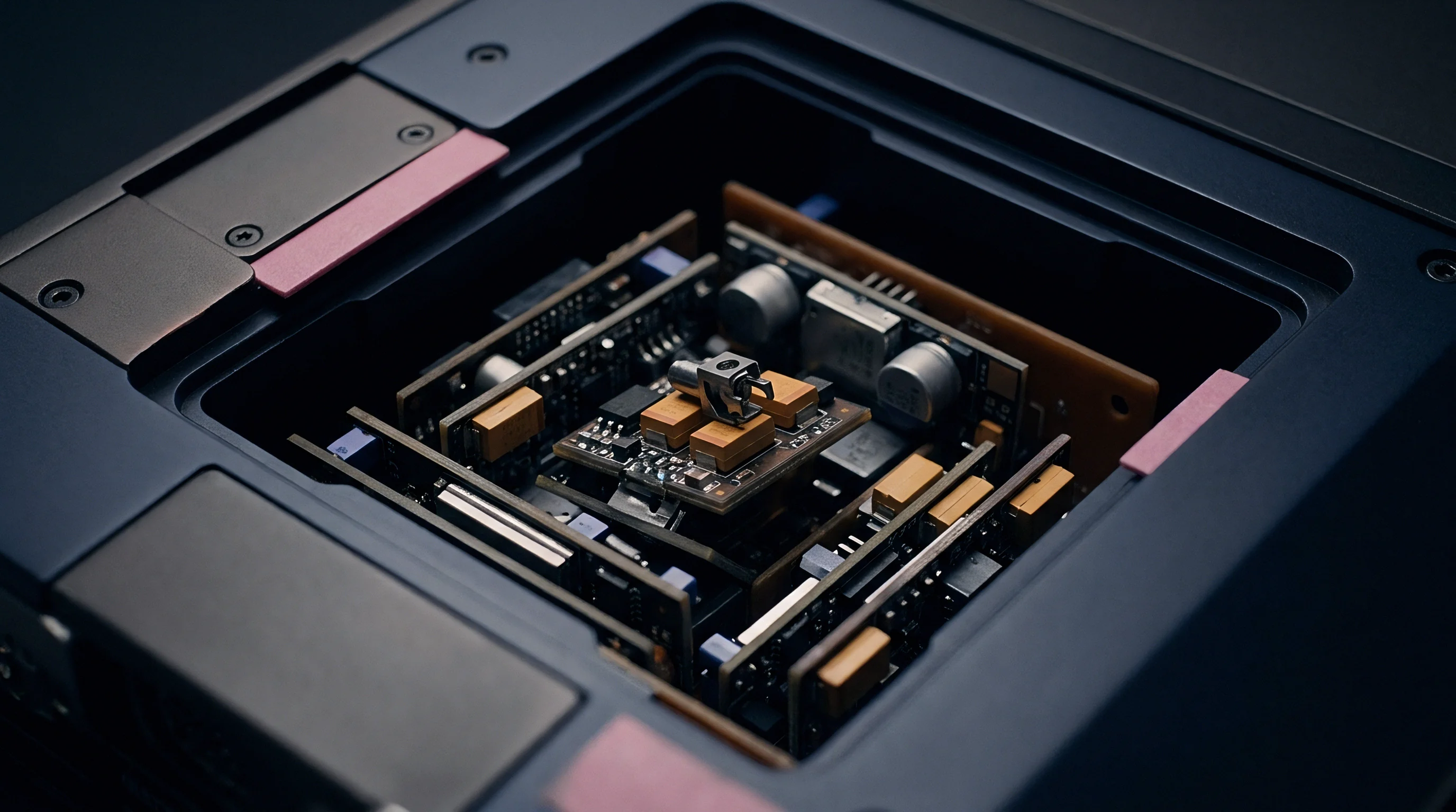
Absorber sheets help suppress these internal resonances. Magnetic absorbers containing carbonyl iron powder give high permeability and loss tangents between 500 MHz and 6 GHz, while carbon-loaded dielectric foams dissipate electric fields through resistive loss. Placing a one-millimeter absorber pad inside the shield lid dampens standing waves, turning RF energy into heat and lowering peak radiated emissions.
Choosing the right shield depends on field impedance, mechanical tolerances, and assembly constraints. Table 2 outlines common containment options used in commercial embedded designs.
| Shielding Mechanism | Material Composition | Thickness Profile | Targeted Spectrum | Practical Attenuation |
|---|---|---|---|---|
| Stamped Surface-Mount Can | Nickel-Silver (Alloy 770) | 0.20 mm | 30 MHz to 6 GHz | 30 to 45 dB |
| Drawn Metal Enclosure | Tin-Plated Mild Steel | 0.35 mm | 10 MHz to 10 GHz | 40 to 60 dB |
| Elastomeric RF Gasket | Ag/Al Filled Silicone | 1.00 to 1.50 mm | 100 MHz to 18 GHz | 50 to 70 dB |
| Magnetic Wave Absorber | Polymer Filled Carbonyl Iron | 0.50 to 1.00 mm | 1 GHz to 12 GHz | 10 to 20 dB loss |
| Conductive Copper Tape | Rolled Copper with Acrylic | 0.07 mm | 100 kHz to 3 GHz | 20 to 35 dB |
Shields also alter thermal management. Enclosing power management ICs or microprocessors inside metal can trap heat. Adding thermal interface materials between components and the shield wall bridges the air gap, transferring heat to the outer surface while preserving RF isolation.
Maintaining effective attenuation instead of causing structural resonance comes down to keeping solid electrical contact along all mechanical joints.

Grant
Modular approvals reduce upfront development risk, but they don’t eliminate testing for the finished product. A module certified under an FCC ID includes grant conditions covering maximum antenna gain, separation distances, and allowed operating modes. Putting a certified Wi-Fi module next to a certified cellular modem in the same enclosure invalidates standalone grant assumptions.
The interaction between host electronics and multiple radiating antennas requires new regulatory evaluation.
Evaluating simultaneous transmission is a legal requirement under FCC Part 2.947 and KDB 996369 D04. When two certified modular radios operate within 20 centimeters of each other, the host integrator must evaluate intermodulation and collocated emissions. Standalone module certifications only prove compliance on a clean reference evaluation board.
Host power supplies, switching circuits, and internal cabling add noise that can push combined emissions past legal limits.
Host Manufacturer Testing Obligations
International regulations divide responsibility between module vendors and host integrators. Under the European Union Radio Equipment Directive 2014/53/EU, the final manufacturer takes full responsibility for overall product compliance. Article 3.1b covers EMC through ETSI EN 301 489-1 and its radio-specific parts, while Article 3.2 governs spectrum use via ETSI EN 300 328 for 2.4 GHz devices and ETSI EN 301 893 for 5 GHz bands.
In the US, strict equipment authorization rules apply. If spurious emissions from a multi-radio host exceed FCC Part 15 Subpart B Class B limits or Part 15 Subpart C radiated limits, the product cannot legally be sold. Fixing parasitic emissions through board revisions or layout changes alters the certified hardware state and triggers additional filing requirements.

Which Permissive Change Covers Radiated Spur Mitigation?
Modifications to a certified radio assembly fall under regulatory filing paths set by FCC Part 2.1043. Adding ferrite clamps, changing enclosure materials, or modifying PCB trace layouts changes field behavior. Table 3 breaks down the verification requirements and regulatory steps for these changes.
| Filing Classification | Mechanical or Circuit Action | Chamber Test Deliverables | Authority Interface | Product Shipping Status |
|---|---|---|---|---|
| Class I Permissive Change | Non-radiating circuit layout shifts | Internal verification test records | None required to FCC | Shipments proceed without delay |
| Class II Permissive Change | Enclosure shifts altering spurious output | Full radiated emissions report | Telecommunication Certification Body | Product held until formal grant |
| Class III Permissive Change | Software-defined radio firmware shifts | Protocol and spectral mask data | Formal FCC direct review | Product held until formal grant |
| New Equipment Grant | Module trace antenna design modification | Complete radio and EMC dossier | TCB grant and new FCC ID | Product held until formal grant |
Host manufacturers follow a set testing sequence before applying compliance marks to commercial products.
- The lab boots the host unit in worst-case concurrent transmit modes while processors execute continuous read-write cycles across system memory.
- Radiated sweeps scan for spurious emissions from 30 MHz up to the tenth harmonic of the highest fundamental frequency.
- Engineers compare intermodulation peaks against the limit lines set by the relevant standards.
- The compliance lead determines whether any margin reduction fits within Class I rules or demands a formal Class II filing.
Failure to verify simultaneous transmission invalidates modular grant protections under FCC KDB 996369 D04 guidance.
Standard commercial warranties limit module compliance guarantees strictly to the bare reference board, ending at the host interface connector.

Ledger
Chamber testing for radiated emissions gets expensive quickly. Accredited labs charge high rates for semi-anechoic chamber access, calibrated receivers, and test staff. A simple pre-compliance scan runs 1,500 to 2,500 dollars per eight-hour shift, while full qualification for a multi-radio device covering FCC Part 15, ISED RSS-247, and RED ETSI requirements routinely costs 15,000 to 35,000 dollars in lab fees alone.
Failing in the chamber multiplies those costs. If a host assembly fails radiated limits at 4.8 GHz during a final compliance run, testing stops on the spot. The lab logs an incomplete test, and the remaining reserved chamber time is lost.
Rebooking an accredited lab typically takes three to six weeks because of limited chamber capacity worldwide, delaying market entry while overhead costs continue to pile up.

Chamber Expenses and Retest Modeling
Tracking the real financial impact of an emissions failure takes clear math. Consider a production run of 10,000 embedded IoT gateways built for global distribution, with 20,000 dollars budgeted for combined FCC and CE lab fees. On initial scans, unmitigated parasitic harmonics coupling into the antenna feed lead to a forty percent failure rate.
A board re-spin triggers immediate costs. Spin four-layer board prototypes, assemble ten validation units, and air-freight them, and you’ve spent 4,500 dollars. Put two senior RF engineers on diagnostics for eighty hours at 120 dollars an hour, and internal labor adds 9,600 dollars.
Rebooking three days of chamber time for diagnostics and retesting costs another 7,500 dollars in lab bills.
The indirect commercial hit is usually much bigger than the lab invoice. A four-week launch delay on a product expected to generate 50,000 dollars in weekly margin means 200,000 dollars in pushed-out gross profit. If that delay misses seasonal retail buying windows, distributors cancel orders entirely.
The total financial loss far outweighs whatever money was saved up front by skipping ground planes or shielding cans.
Global deployment strategies also have to factor in regional approval requirements. Japan MIC certification under the Radio Act requires strict verification of spurious emissions under Giteki rules. South Korea’s National Radio Research Agency requires testing inside accredited domestic labs, while Brazil’s ANATEL mandates local sample testing and ongoing certificate renewals.
Catching an unmitigated clock harmonic in an overseas lab invalidates previous domestic filings and resets testing timelines across all target markets at once.
Setting up bench-top pre-compliance testing prevents expensive surprises in the chamber. A three thousand dollar investment in an entry-level spectrum analyzer, near-field probe set, and RF isolation tent catches mixed-frequency spurs before booking lab time. Fixing trace routing during schematic capture costs almost nothing, whereas reworking thousands of assembled boards in a warehouse means manual teardowns, hand-soldered shields, and heavy write-downs.
Under standard commercial supply agreements, the integrator bears full financial liability for host-level radiated emissions non-compliance.